[ad_1]
An idea developed on the Nationwide Renewable Vitality Laboratory (NREL) simplifies the method to fabricate perovskite photo voltaic cells, which may speed up
the trail towards commercialization of the expertise.
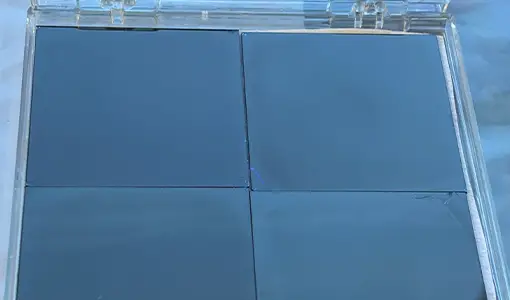
Perovskite photo voltaic cells are made by sequentially depositing varied layers onto a conductive
glass substrate, requiring a number of coatings to create the required full gadget construction.
The brand new method eliminates or combines a few of these steps, thereby simplifying
the manufacturing course of, which may result in but decrease manufacturing prices.
NREL researchers have been in a position to make these high-efficiency perovskite photo voltaic cells with out
sure steps.
Perovskite photo voltaic cells are composed of a perovskite light-absorbing layer and adjoining
layers that extract constructive and unfavorable fees on reverse sides of the perovskite
when gentle is absorbed. Considered one of these layers, referred to as the hole-transport layer (HTL),
is used to extract constructive fees. Perovskites might be made with out an HTL, however such
gadgets’ effectivity lags that of the total perovskite photo voltaic cell gadget buildings.
The group produced a high-efficiency photo voltaic cell that retained greater than 90% of the
preliminary effectivity after 1,200 hours of steady operation.
Xiaopeng Zheng, a postdoctoral researcher within the Chemistry and Nanoscience Middle
at NREL, stories in Nature Vitality how a one-step solution-coating process allowed two separate layers, particularly the
HTL and perovskite absorber, of a photo voltaic cell to spontaneously type with just one coating
step, eliminating the separate hole-transport layer fabrication. As an alternative, because the paper
factors out, the chemical options type “a strong self-assembled monolayer concurrently
as a superb hole-selective contact whereas the perovskite crystallizes.”
Zheng stated the brand new, simplified course of to make the HTL and perovskite concurrently
reduces the variety of coating and heating steps and removes the necessity for costly
HTL supplies.
“It’s difficult to uniformly manufacture a skinny HTL layer utilizing the scalable resolution
methodology, and this can be additionally a barrier to commercialization,” Zheng stated. “Our method
may additionally keep away from this drawback.”
He estimated that eradicating the steps beforehand wanted to create the HTL after which
having to warmth it up may minimize the solution-processing time by a 3rd.
“Even when we didn’t save loads of time right here, it brings concerning the notion that the manufacturing
course of may very well be reevaluated with this new idea in thoughts,” stated Joseph Luther, a
corresponding writer of the paper and senior analysis fellow inside the Supplies,
Chemical, and Computational Science directorate at NREL. “A number of processing steps may very well be mixed; layers may spontaneously type. I’m
not but positive how one may coat all of the layers without delay, however this highlights that maybe
it may very well be performed.”
Along with Zheng and Luther, the paper, “Co-deposition of Hole Selective Contact and Absorber for Improving the Processability
of Perovskite Solar Cells,” was co-authored by NREL colleagues Min Chen, Chuanxiao Xiao, Jay Patel, Darius
Kuciauskas, Rebecca Scheidt, Steven Harvey, Brian Wieliczka, Ahmad Kirmani, and Michael
McGehee.
Different researchers are from Hong Kong, Switzerland, and Lithuania, in addition to from
the College of Kentucky, the College of Toledo, and Brown College.
“Whereas the preliminary discovery of the process was made at NREL, the co-authors from
varied different establishments discover the identical results and strengthened the findings,” Zheng
stated. “We found and proved the idea at NREL, and fairly a couple of different teams
expanded this discovering to be extra common with totally different perovskite compositions,
HTLs, totally different solvents and varied different coating kinds. Such coordinated efforts
are welcomed within the perovskite subject. We imagine it will enable this work to realize
better adoption.”
Understanding how the totally different layers crystallize was supported by the Middle for
Hybrid Natural-Inorganic Semiconductors for Vitality (CHOISE), an Vitality Frontier Analysis
Middle funded by the U.S. Division of Vitality’s Workplace of Primary Vitality Sciences,
and the manufacturability and scaling work was supported by the division’s Photo voltaic
Vitality Applied sciences Workplace.
[ad_2]
Source link